
Table of Contents
1. Introduction: The Promise of Graphene
2. Breaking the Barrier: Graphene’s Semiconductor Functionality
3. How Graphene Transistors Differ from Silicon
4. Implications for the Electronics Industry
5. Challenges Ahead and Research Directions
1. Introduction: The Promise of Graphene
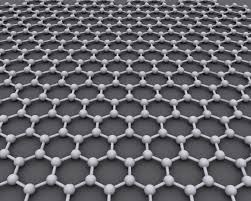
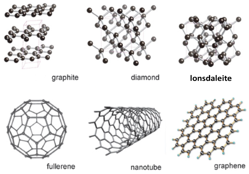
Since its isolation in 2004, graphene has captivated the scientific and industrial communities with its remarkable properties. As a single layer of carbon atoms arranged in a two-dimensional honeycomb lattice, graphene exhibits extraordinary electrical conductivity, mechanical strength, and thermal efficiency. Yet, despite its promise, one critical property has long been missing: the ability to behave as a semiconductor. Semiconductors form the core of modern electronics — from microprocessors and memory chips to LEDs and solar cells. For graphene to replace silicon in these applications, it had to be more than just conductive; it had to allow precise control of electrical current — in other words, it needed a bandgap.
Researchers have spent over a decade trying to induce a bandgap in graphene without destroying its conductive properties. The lack of this bandgap has prevented graphene from being used as a functional transistor material in practical electronic devices. However, recent developments have finally achieved this long-sought goal, creating a functional graphene semiconductor that maintains its hallmark advantages. This breakthrough not only brings graphene back into the spotlight but sets the stage for a fundamental transformation in electronic design and manufacturing.
2. Breaking the Barrier: Graphene’s Semiconductor Functionality
The most critical obstacle in making graphene a viable semiconductor was its intrinsic zero bandgap — it behaves more like a metal than a silicon-based semiconductor. A semiconductor needs a tunable bandgap to function effectively in digital circuits, allowing transistors to switch on and off. Achieving this in graphene required either modifying its structure or creating new heterostructures involving other 2D materials.
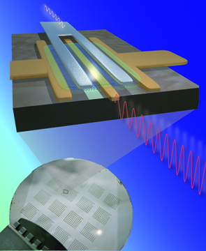
Recent advances have made this possible. A team of international scientists successfully engineered a graphene-based material with an effective bandgap by using a technique called nano-ribbon fabrication, where graphene is sliced into narrow strips just a few nanometers wide. This quantum confinement forces electrons to behave differently, effectively creating a usable bandgap while retaining graphene's conductivity. In parallel, other teams have used graphene/hBN (hexagonal boron nitride) heterostructures and chemical doping to induce semiconducting behavior.
These achievements were validated through experimental setups demonstrating transistor-like switching behavior, low leakage currents, and high electron mobility — all hallmarks of a functioning semiconductor. This success lays the groundwork for graphene-based logic circuits and other key components of future electronics.
3. How Graphene Transistors Differ from Silicon
Silicon has dominated the semiconductor world for decades due to its abundance, well-understood fabrication processes, and reliable semiconducting behavior. However, silicon is reaching its physical and performance limits, especially as devices shrink to the nanoscale. Graphene-based transistors offer a compelling alternative, especially in performance-critical and energy-sensitive applications.
Graphene transistors exhibit exceptionally high carrier mobility, which enables electrons to move through the material with minimal resistance. This means that graphene transistors can potentially operate at much higher frequencies than silicon-based ones, translating to faster data processing and reduced energy loss. Additionally, graphene’s flexibility and strength make it ideal for applications in wearable tech, foldable displays, and flexible circuits — areas where silicon struggles.
That said, the production of graphene transistors is currently more complex and costly. Unlike silicon, which has an extensive industrial ecosystem, graphene is still emerging in terms of scalable, defect-free manufacturing. Yet the efficiency, speed, and thermal performance gains graphene offers could eventually offset the higher costs as fabrication methods improve.
4. Implications for the Electronics Industry
With functional graphene semiconductors now a reality, the electronics industry stands on the verge of a major disruption. This development could catalyze a shift away from silicon-based electronics toward 2D-material-based devices, especially in high-frequency, high-efficiency, or ultra-compact applications. Industries like telecommunications, artificial intelligence, quantum computing, and aerospace electronics are already exploring prototypes that leverage graphene’s speed and thermal resilience.
Moreover, the integration of graphene with existing silicon technologies — rather than outright replacement — is a more immediate and realistic approach. Hybrid graphene-silicon circuits could optimize performance while taking advantage of existing manufacturing infrastructure. Companies investing in R&D for graphene electronics today may find themselves holding key patents and capabilities as the material transitions from the lab to commercial applications.
Global market analysts project that the graphene electronics market could exceed billions in value by the early 2030s, driven by innovations in consumer electronics, sensors, and next-generation communication devices like 6G networks. The race is on to build scalable, affordable, and efficient graphene-based components that can meet commercial demand.

5. Challenges Ahead and Research Directions
Despite the breakthrough, there are significant hurdles to overcome before graphene semiconductors become mainstream. First and foremost is manufacturing at scale. Producing high-quality, uniform graphene at industrial volumes remains a challenge, particularly for nano-ribbon structures. Additionally, integrating graphene components into existing silicon-based chips requires precise alignment, clean interfaces, and new fabrication techniques.
Another key challenge is thermal management. While graphene conducts heat exceptionally well, managing that heat at the device level — especially in densely packed circuits — still requires advanced cooling solutions. There are also standardization and reliability concerns, particularly in mission-critical applications where long-term stability is essential.
On the research front, scientists are exploring multi-layer graphene systems, twisted bilayer graphene, and graphene oxide to fine-tune electronic properties and unlock new functionalities. There is also considerable interest in combining graphene with other 2D materials like MoS₂ to create van der Waals heterostructures, offering tailored properties for specific applications.

You must be logged in to post a comment.